VCSEL
Vertical-cavity surface-emitting lasers, characterized and qualified in-house. This is the one area where we publish performance results and where product is available today.
Readout
Wavelength
A vertical-cavity surface-emitting laser is the pump source at the centre of a vapor cell sensor. For a rubidium-referenced sensor the number that matters is the rubidium D1 line at 794.98 nm, and our 25 µm mesa, 3 µm aperture devices are built to sit close to it — an etalon check across characterized samples reads 791.5 nm, and thermal tuning moves a single device from 791.035 nm at 24.07°C to 791.315 nm at 30°C. Devices are qualified across a 25°C to 80°C envelope at 0.8, 1.5 and 2.2 mA drive.
A separate, higher-power line of multijunction VCSELs runs at 905 nm and 940 nm for automotive sensing — the same process, a different application and a different target wavelength than the rubidium-referenced devices above.
Characterization
Measured, not assumed
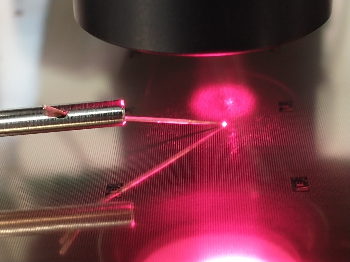
Every die is probed and scanned on an automated setup rather than sampled by hand. That is what makes a wavelength figure a specification instead of a typical value, and it is the same apparatus that supports precise photonic characterization for the rest of the sensor.
The photograph is the measurement in progress: two probes down on a single die, the emitted beam visible on the wafer surface.